


“OptaScan gebruikt de Xignal muizenvallen al enige jaren, niet omdat we korter bij onze klanten (grote levensmiddelenbedrijven) willen zijn, maar omdat we juist méér tijd willen besteden aan het structureel voorkómen en oplossen van problemen met plaagdieren. De Xignal vallen sluiten daarom heel goed aan bij de plaagdierbeheerssystemen van OptaScan”.

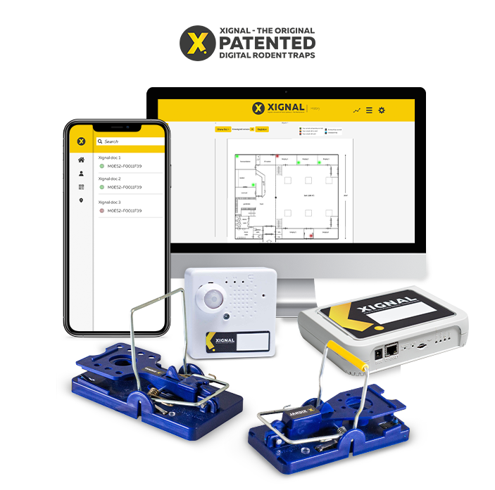
“In de digitalisering van de plaagdierbranche loopt Dimo Systems met Xignal voorop. Het is een relevante meerwaarde 24/7 informatie te kunnen ontvangen. Dit draagt bij aan een effectief en professioneel beheersplan. De ontwikkelingen gaan door en ik ben verheugd om onze klanten goed te kunnen informeren op het gebied van digitale plaagdierbestrijding.”

"De producten van Xignal zijn van toegevoegde waarde voor ASB Plaagdierbeheersing omdat het een andere manier van denken en een nieuwe efficiënte manier van werken biedt. Klanten zijn beter gediend door de vele voordelen die het systeem biedt. U kunt 24/7, 365 dagen per jaar sneller reageren op wat er speelt. Dit vermindert de economische schade en eventuele overlast aanzienlijk, omdat u direct kunt reageren op elke melding. Onze klanten zijn blij met Xignal en wij, ASB Plaagdierbeheersing zijn goed voorbereid op de toekomst."